


 12 / 84

LatestNews
Advantest Unveils New Pick-and-Place IC Handler to Improve
Efficiency in High-Volume Semiconductor Manufacturing and Device
Characterization
Leading
semiconductor
test
equipment supplier Advantest
Corporation (TSE: 6857) has
introduced its M4872 pick-and-place
handler to improve productivity in
testing system-on-chip (SoC) devices
in high-volume manufacturing
(HVM) and device characterization
pre-production environments. This
helps users to keep pace with the
rapidly changing SoC market and
quickly adapt to changes in device
technology.
The new handler matches all of
the leading-edge performance
specifications of its predecessor, the
M4871 handler, including throughput
of up to 15,000 units per hour, in a
footprint that is approximately 10 percent smaller. The portable
M4872 handler has advanced vision-alignment capabilities and
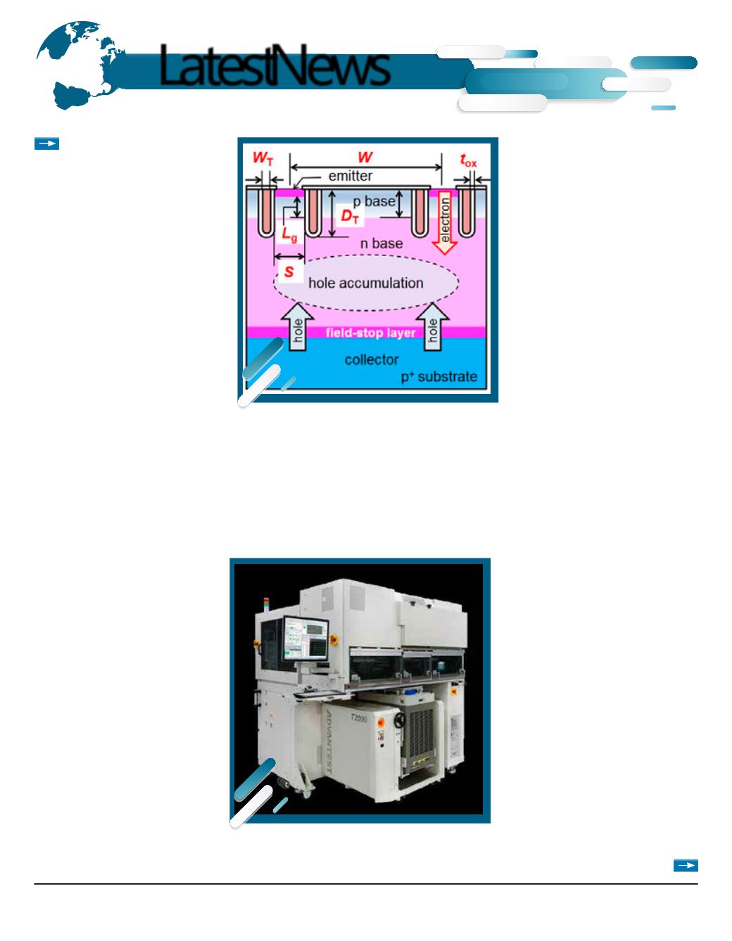
they also reduced the trench
depth by 1/k. Although this
has a slightly negative effect on the
IE effect, it has considerable benefits
for fabrication ease and cost and
the dependence of (Vce(sat)) on
the trench depth was deemed to
be small. The gate voltage was also
decreased by a factor of 1/k, while
the cell pitch was maintained at 16
μm.
Reference
K. Kakushima1, T. Hoshii1, K. Tsutsui1,
A. Nakajima2, S. Nishizawa2, H.
Wakabayashi1, I. Muneta1, K. Sato3,
T. Matsudai4, W. Saito4, T. Saraya5,
K. Itou5, M. Fukui5, S. Suzuki5,
M. Kobayashi5, T. Takakura5, T. Hiramoto5, A. Ogura6,
can accommodate an optional active
thermal control system.
The vision alignment-equipped M4872
incorporates a common change kit,
which saves time and money as well as
helps to safeguard devices under test
from potentially damaging package.
Using a common change kit also
significantly shortens time to market.
In total, the time it takes to change
device types is reduced by more than
45 percent, enabling nearly twice the
throughput of handlers that rely on
standard change kits.
By using Advantest’s on-the-fly vision-
alignment technology, devices under
test can be precisely positioned,
making the new handler ideally suited
for testing fine-pitch ICs and devices with both top- and bottom-
side contacts. The resulting improvements in test yields
Y. Numasawa6, I. Omura7, H.
Ohashi1, and H. Iwai1, Experimental
verification of a 3D scaling principle
for low Vce(sat) IGBT, Technical
Digest of IEDM2016, Session 10.6,
(2016),
http://ieee-iedm.org/1. Tokyo Inst. of Technology,
Yokohama, Japan
2. Nat. Inst. Advanced Industrial
Science and Technology, Tsukuba,
Japan
3. Mitusbishi Electric, Fukuoka,
Japan
4. Toshiba Corp., Tokyo, Japan
5. The University of Tokyo, Tokyo,
Japan
6. Meiji University, Kawasaki, Japan
7. Kyushu Inst. of Technology, Kitakyushu, Japan
12 l New-Tech Magazine Europe